

MONOSTABLE OPERATION OF 555IC

The circuit triggers on a negative going input signal when the level reaches (1/3).VCC. Once triggered the circuit will remain in this state until the set time is elapsed, even if it is triggered again during this interval.
The time that the output is in the high state is given by t= 1.1.RTCT. Applying a negative pulse simultaneously to the reset terminal (pin 4) and the trigger terminal (pin 2) during the timing cycle, discharges the external capacitor CT and causes the cycle to start over again. The timing cycle will now commence on the positive edge of the reset pulse. During the time the reset pulse is applied, the output is driven to its low state. When the reset function is not in use, it is recommended that it be connected to VCC to avoid any possibility of false triggering.

ASTABLE OPERATION OF 555IC
The circuit shown in the Figure, will trigger itself and free run as a multi-vibrator. The external capacitor charges through RA and RB and discharges through RB only. Thus the duty cycle may be set precisely by the ratio of these two resistors.

In this mode of operation, the capacitor charges and discharges between (1/3).VCC and (2/3).VCC. As in the triggered mode, the charge and discharge times and hence the frequency independent of the supply voltage.

The charge time (output high) is given by:
t1 =0.693 (RA + RB) CT
The discharge time (output low) is given by :
t2=0.693 (RB) CT
thus the total period T is given by :
T = t1+t2 = 0.693 (RA+2 RB) CT,
and the frequency of oscillation is then:
f = 1/T
This may be easily found by the graph shown below,

The duty cycle is given by,
D= RB /(RA + 2RB) .
From the above equation, it will be seen that the frequency and the duty cycle are inter-dependent and change of value of RA or RB affects both. It is possible to have a completely independent control of the charge and discharge times by using two external diodes as shown in figure below.

The timing capacitor CI charges through DI and RI and discharges through D2 and R2.
A modified arrangement shown, provides a control over duty cycle without changing the output pulse frequency. The diode voltage drops, however, make the time more sensitive to supply voltage variations.
BISTABLE OPERATION OF 555IC
The 555 timer can also function as a bistable flip-flop in such applications as TTL compatible drivers. This flip-flop offers the advantage that it operates from many different supply voltages, uses little power and requires no external components other than bypass capacitors in noisy environments. It also provides a direct relay driving capability.
As shown in Figure, a negative pulse applied to the trigger input terminal (Pin2) sets the flip flop and the output Q goes high. A positive going pulse applied to threshold terminal will reset the flip-flop and drive the Q output low. The flip-flop can also be reset by applying a negative going pulse to the reset terminal (Pin 4). In this mode Pin 6 is kept low.
SCHMITT TRIGGER USING 555IC

A sine wave input of sufficient. amplitude to exceed the reference levels causes the internal flip-flop to be set and reset. In this way, it creates a square wave at the output. So long as R1 is equal to R2; the 555IC will be automatically biased correctly for almost any supply voltage. The output waveform is 180 degree our of phase with the applied sine wave. The circuit can be used as a signal shaper/buffer with advantage of availability of high output current.
By modifying the input time constant of the circuit shown (e.g., reducing the value of input capacitor to .001uF) so that the input pulses get differentiated, the arrangement can also be used either as a bistable device or to invert pulse waveforms, In the later case, the fast time constant of the. combination of Cl with Rl and R2 causes only the edges of the input pulse or rectangular waveform to be passed. These pulses set and reset the flip-flop and a high level inverted output is the result.
SQUARE WAVE OSCILLATOR USING 555IC
A Square waves can be obtained by using 555 timer IC by the circuit as shown in the figure below,
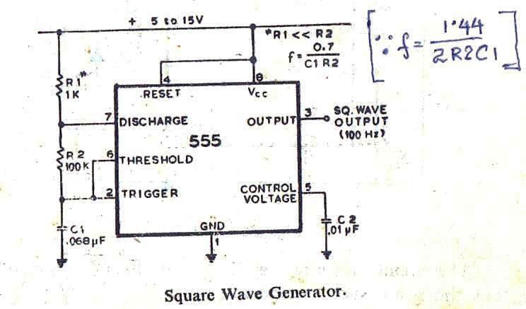
The asymmetry of a conventional astable circuit is a !result of the fact that charging and discharging times are not equal. In the circuit shown the capacitor Cl is charged through RI and R2 while discharged through R2. If Rl is made very small compared to R2, the.both time constant will be reduced so that they essentially depend on R2 and Cl, The frequency of operation (f) IS approximately 0.7/(R2C1).
The frequency is of course independent to the supply voltage.

The circuit shown in Figure is useful for providing controlled 'on' times for such equipment as photo-enlargers, developers, small heaters, incandescent lamps, etc. Time is set by potentiometer R2 which provides a range of 1 sec. to 100 second with timing capacitor CI of 100 µF.
The output at pin 3 is normally low and the relay is held off. A momentary touch on switch Sl energizes the relay which is held closed for a time 1.1 x (R1 + R2). C1 and then released. The exact length of the timing interval will depend on the actual capacitance of Cl. Most electrolytic capacitors are rated on the basis of minimum guaranteed value and the actual value may be higher. The circuit should be calibrated for various positions of the control knob of R2 after the timing capacitor has had a chance to age. Once the capacitor has reached its stable value, the timings provided should be well within the photographic requirements.


Touch the small metal plate and the relay gets energized, kept on for about 100 seconds and then released. Such circuits are ideally suited for making touch-operated call-bells, buzzers or small toys which, once touched, operate for a small time and then switch off automatically.
The input impedance of the trigger comparator of 555 is very high and the circuit can be triggered by the voltage induced in a human body. This fact is used in making the touch switch shown in Figure. Toy motors can be driven directly by deleting the diodes D1, D2 and the relay and driving a power transistor like AC 128 directly from the output pin 3 of the IC.

Photo Timer.

The output at pin 3 is normally low and the relay is held off. A momentary touch on switch Sl energizes the relay which is held closed for a time 1.1 x (R1 + R2). C1 and then released. The exact length of the timing interval will depend on the actual capacitance of Cl. Most electrolytic capacitors are rated on the basis of minimum guaranteed value and the actual value may be higher. The circuit should be calibrated for various positions of the control knob of R2 after the timing capacitor has had a chance to age. Once the capacitor has reached its stable value, the timings provided should be well within the photographic requirements.

Touch Plate Controller

Touch the small metal plate and the relay gets energized, kept on for about 100 seconds and then released. Such circuits are ideally suited for making touch-operated call-bells, buzzers or small toys which, once touched, operate for a small time and then switch off automatically.
The input impedance of the trigger comparator of 555 is very high and the circuit can be triggered by the voltage induced in a human body. This fact is used in making the touch switch shown in Figure. Toy motors can be driven directly by deleting the diodes D1, D2 and the relay and driving a power transistor like AC 128 directly from the output pin 3 of the IC.

AUTO WIPER CONTROL

Basically the circuit is an astable multivibrator, in which the output level at pin 3 remains high for a long time decided by R2 and low for a short time decided by R3. The low going output at pin 3 drives the wiper motor via Tl and T2 for a time just sufficient to operate the parking switch. The wipers then make one sweep and rest again in their normal parked position till the next pulse. Resistor R5 limits the current and power dissipation in Tl. Transistors Tl and T2 may be replaced by a relay if desired.

AUTOMATIC HEADLIGHT TURN-OFF


TINY FLASHER


