Drop Down MenusCSS Drop Down MenuPure CSS Dropdown Menu
Showing posts with label Projects & Principles. Show all posts

Sunday, 13 September 2015

PROJECTS USING 555IC

WARBLE TONE GENERATOR

 The tone generator described here is an audio attention gene­rator. Such circuits may be used for alarm sirens or for producing unique tones in 'cable testing, which will not get mixed up with other noises. 

In the schematic shown in figure, the first 555 oscillates below 10 Hz. Its rectangular output is filtered by filter R3, R4 and C3 to produce triangular waves which modulate the 1 kHz oscillator using the, second 555 in astable mode. The exact frequency, rate and deviation of the circuit can be easily modified to produce almost any type of warble sound. The output may be amplified by an audio amplifier to the required power level.

LINEAR SAW TOOTH GENERATOR

The voltage across the timing capacitor CT in the mono­stable multivibrator circuit, rises to 2/3VCC and then drops to almost zero. A sawtooth waveform is, therefore, available across this capacitor, but is not linear because the capacitor voltage rises exponentially. In figure shown above, the capacitor is allowed to charge via a constant current source comprising of T1, RI, R2, R3 and R4. The voltage now rises linearly and the output is taken via an emitter follower buffer stage T2 to isolate the load from the timing circuit. For use as a scope time base, a trigger signal may be applied to terminal 2 of the IC. 

Another arrangement by which a linear sawtooth can be produced is by bootstrapping the output as shown in figure, Capa­citor C1 begins to charge through R1, R2, and R3 towards VCC. The voltage across R5 at the output of emitter follower T1 is almost same as that at pin 7 of the IC. This voltage is fed back to junction of R1 and R2. As a result, the voltage across R2 remains essentially constant during C1's charging cycle and the capacitor voltage rises linearly. Connecting pin 2 to pin 6 causes the circuit to trigger itself and free run as an astable multivibrator.
Alternatively, the synchronizing signal may be applied to pin 2.
Resistor R3 is required to slow down the negative discharge slope of the saw tooth. R3.C1 is kept greater than 5 micro
-seconds.

SQUARE WAVE GENERATOR

With only one external resistor and one capacitor and a 555 timer IC, can be made to generate fairly accurate square waves. 

The square wave generator circuit shown in figure makes use of the fact that output voltage in a 555 IC is 180
0 out of phase with the capacitor voltage. To understand the circuit operation let us assume a state when output is high and the capacitor C1 is charging via R1. When the voltage across capacitor reaches 2/3VCC, the output goes low and C1 now starts discharging through R1. When the voltage across C1 falls to 1/3VCC, the circuit trips again, output goes high, the capacitor starts charging and the cycle repeats endlessly. Since charging and discharging takes through R1 only, the output is a symmetrical square wave. The period of oscillator is given by T= 1.4RC, F=1/T.

The output symmetry depends on the accuracy of the timer's internal resistor string which produces the IC's comparator reference voltages. These errors can be eliminated by adding a trimming resistor R2 and connecting it to supply line or ground depending on the correction needed.

SENSE OF TIME TESTER

How accurate is your sense of time? You can find it out for yourself by catching a flashing LED. 

When S2 is on, the circuit in Figure, operates as an astable multivibrator and the LED is lit for about 0.1 sec flashing every 1.5 seconds. Since the human reaction time is more then this, you cannot catch it once it is seen on, by pressing S1. If your sense of time interval is good. and you press S1 within that 0.1 Sec, the discharging of C1 stops and the lamp stays lit. You may change the ON and OFF periods by changing R1 and R2 or C1 to suit your convenience.


SOLID STATE FLASHER


 The mains operated flasher shown in figure, uses a 555 IC timer to control the ON and OFF times of a triac which controls power to the load. The power supply for the IC is obtained by half wave rectifier and a stabilizer circuit comprising of rectifier diode D1, zener diode D2, resistor R1 and filter capacitor C1. The lamp in the load circuit remains on for about 1 second and off for about 0.7 seconds. Other timings may be obtained by choosing appropriate R2 and R3.

Saturday, 5 September 2015

Kirchhoff’s Voltage, Current Law & Superposition Principle

Kirchhoff’s Voltage Law

Kirchhoff’s voltage law (often abbreviated KVL) states that the sum of voltages around any closed loop in a circuit must be zero.
In essence, this law expresses the basic properties that are inherent in the definition of the term “voltage” or “electric potential.” Specifically, it means that we can definitively associate a potential with a particular point that does not depend on the path by which a charge might get there. This also implies that if there are three points (A, B, and C) and we know the potential differences between two pairings (between A and B and between B and C), this determines the third relationship (between A and C).
Without thinking in such abstract and general terms, we apply this principle when we move from one point to another along a circuit by adding the potential differences or voltages along the way, so as to express the cumulative voltage between the initial and final point. Finally, when we go all the way around a closed loop, the initial and final point are the same, and therefore must be at the same potential: a zero difference in all.
The analogy of flowing water comes in handy. Here, the voltage at any given
point corresponds to the elevation. A closed loop of an electric circuit corresponds to a closed system like a water fountain. The voltage “rise” is a power source—say, a battery—that corresponds to the pump. From the top of the fountain, the water then flows down, maybe from one ledge to another, losing elevation along the way and ending up again at the bottom. Analogously, the electric current flows “down” in voltage, maybe across several distinct steps or resistors, to finish at the “bottom” end of the battery. This notion is illustrated by in the simple circuit in Figure below, that includes one battery and two resistors.


Note that it is irrelevant which point we choose to label as the “zero” potential: no matter what the starting point, adding all the potential gains and drops encountered throughout the complete loop will give a zero net gain.

Kirchhoff’s Current Law

Kirchhoff’s current law (KCL) states that the currents entering and leaving any
branch point or node in the circuit must add up to zero.

This follows directly from the conservation property: electric charge is neither created nor destroyed, nor is it “stored” (in appreciable quantity) within our wires, so that all the charge that flows into any junction must also flow out. Thus, if three wires connect at one point, and we know the current in two of them, they determine the current in the third.
Again, the analogy of flowing water helps make this more obvious. At a point
where three pipes are connected, the amount of water flowing in must equal the amount flowing out (unless there is a leak). For the purpose of computation, we assign positive or negative signs to currents flowing in and out of the node, respectively.
It does not matter which way we call positive, as long as we remain consistent in our definition. Then, the sum of currents into (or out of) the node is zero. This is illustrated with the simple example in Figure below, where KCL applied to the branch point proves that the current through the battery equals the sum of currents through the individual resistors.


The Superposition Principle

This principle applies to circuits with more than one voltage or current source. It states that the combined effect—that is, the voltages and currents at various locations in the circuits—from the several sources is the same as the sum of individual effects.
Knowing this allows one to consider complicated circuits in terms of simpler components and then combining the results. In power systems, the superposition principle is used to conceptualize the interactions among various generators and loads. For example, we may think of the current or power flow along a transmission link due to a “shipment” of power from one generator to one consumer, and we add to that the current resulting from separate transactions in order to obtain the total flow on that link. With voltages held fixed, the currents become synonymous with power flows, and we can add and subtract megawatt flows superimposed along various transmission links.
For a simple example where we can deal with currents and voltages explicitly,
consider the circuit in Figure below.


This circuit has two power sources. The first source, labeled S1, is a battery that functions as a voltage source, delivering 12 volts. The second source, S2, is a current source that delivers 1.5 amperes. This type of source is less familiar in power systems than in electronics; it has the property of always delivering a specific current regardless of the resistance in the circuit connected to it, while allowing the voltage at its terminals to vary (as
opposed to the more familiar voltage source that specifies terminal voltage while the current depends on resistance in the circuit). We introduce the current source here because it makes for a good illustration of the superposition principle.
Suppose we wish to predict the voltage level v and current i at the locations identified in the diagram. It is not immediately obvious what the voltages and currents at various points in this circuit should be as a result of the combination of the two sources. The superposition principle is an indispensable analytic tool here: it states that we can consider separately the voltage and current that would result from each individual source, and then simply add them together. This principle applies regardless of the circuit’s complexity or the number of power sources; it also holds true at any given instant in a circuit with time-varying sources.
In our example, the voltage v that would result from only S1—written as v(S1), indicating that v for now is only a function of S1—is determined from the relative magnitudes of the two resistances in the circuit, R1 and R2, while ignoring the presence of the current source.

Since R2 at 2Ω represents one-third of the total resistance in this simple series circuit, 2Ω + 4Ω, the voltage across R2 that we want to find is simply one-third of the total:

v(S1) = 12V.2Ω/(4Ω + 2Ω) = 12V.1/3 = 4V

Ignoring the current source technically means setting the current through it to zero, or replacing it with an open circuit. Having gotten rid of the extra circuit branch, the current i(S1) through the resistor R2 that would result from S1 alone is easy to find with Ohm’s law:

i(S1) = 12V/(4Ω + 2Ω) = 2A

Next, we ignore the voltage source, meaning that we set the voltage difference across it to zero, or replace it with a short circuit.

The current i(S2) through R2 based on the current source alone is found from the relative magnitudes of the resistances in each branch: since R2 has half the resistance of R1, twice the current will flow through it, or two thirds of the total:

i(S2) = 1.5A.4Ω/(4Ω + 2Ω) = 1.5A.2/3 = 1A

The voltage v(S2) due to the current source alone is again found via Ohm’s law:


v(S2) = 1A.2Ω = 2V

We can now superimpose the contributions from the two sources and find:


v= v(S1) + v(S2) = 4V + 2V = 6V, and

i = i(S1) + i(S2) = 2A + 1A = 3A
 
Although this simple example could have been solved without the use of superposition, the technique is vital for analyzing larger and more complex circuits, including those with time-varying sources.


Saturday, 29 August 2015

555IC AND ITS USES

MONOSTABLE OPERATION OF 555IC

In this mode of operations the timer acts as a one shot. Details of the external connections and the wave-forms are shown in Figure below. The external timing capacitor CT is held initially dis­charged by the transistor inside the timer. Upon application of a negative pulse to pin 2, the flip-flop is set which releases the short circuit across the external capacitor and drives the output high. The voltage across the capacitor, now, rises ex­ponentially with the time constant RT.CT. When the voltage across the capacitor equals (2/3).VCC, the threshold comparator resets the flip-flop which, in turn, discharges the capacitor rapidly and drives the output to its low state. The circuit rests in this state till the arrival of next pulse.


The circuit triggers on a negative going input signal when the level reaches (1/3).VCC. Once triggered the circuit will remain in this state until the set time is elapsed, even if it is triggered again during this interval.
The time that the output is in the high state is given by t= 1.1.RTCT. Applying a negative pulse simultaneously to the reset terminal (pin 4) and the trigger terminal (pin 2) during the timing cycle, discharges the external capacitor CT and causes the cycle to start over again. The timing cycle will now commence on the positive edge of the reset pulse. During the time the reset pulse is applied, the output is driven to its low state. When the reset function is not in use, it is recommended that it be connected to VCC to avoid any possibility of false triggering.

ASTABLE OPERATION OF 555IC


The circuit shown in the Figure, will trigger itself and free run as a multi-vibrator. The external capacitor charges through RA and RB and discharges through RB only. Thus the duty cycle may be set precisely by the ratio of these two resistors.

In this mode of operation, the capacitor charges and discharges between (1/3).VCC and (2/3).VCC. As in the triggered mode, the charge and discharge times and hence the frequency independent of the supply voltage.

The charge time (output high) is given by:

t1 =0.693 (RA + RB) CT

The discharge time (output low) is given by :

t2=0.693 (RB) CT

thus the total period T is given by :

T = t1+t2 = 0.693 (RA+2 RB) CT,

and the frequency of oscillation is then:

f = 1/T 

This may be easily found by the graph shown below,

The duty cycle is given by,

D= RB /(RA + 2RB) .

From the above equation, it will be seen that the frequency and the duty cycle are inter-dependent and change of value of RA or RB affects both. It is possible to have a completely independent control of the charge and discharge times by using two external diodes as shown in figure below.

The timing capacitor CI charges through DI and RI and discharges through D2 and R2.


 A modi­fied arrangement shown, provides a control over duty cycle without changing the output pulse frequency. The diode voltage drops, however, make the time more sensitive to supply voltage variations.

BISTABLE OPERATION OF 555IC

The 555 timer can also function as a bistable flip-flop in such applications as TTL compatible drivers. This flip-flop offers the advantage that it operates from many different supply voltages, uses little power and requires no external components other than bypass capacitors in noisy environments. It also provides a direct relay driving capability.


As shown in Figure, a negative pulse applied to the trigger input terminal (Pin2) sets the flip flop and the output Q goes high. A positive going pulse applied to threshold terminal will reset the flip-flop and drive the Q output low. The flip-flop can also be reset by applying a negative going pulse to the reset terminal (Pin 4). In this mode Pin 6 is kept low.

SCHMITT TRIGGER USING 555IC

The two comparators of the 555 timer can be used independently as a Schmitt trigger, as shown in figure. The two com­parator inputs (Pin 2 and 6) are tied together and biased at (1/2)VCC through a voltage divider Rl and R2. Since the threshold com­parator will trip at (2/3)VCC and the trigger comparator will trip at  (1/3)VCC, the bias provided by the resistors Rl and R2 is centered within the comparators' trip limits.


A sine wave input of sufficient. amplitude to exceed the reference levels causes the internal flip-flop to be set and reset. In this way, it creates a square wave at the output. So long as R1 is equal to R2; the 555IC will be automatically biased correctly for almost any supply voltage. The output waveform is 180 degree our of phase with the applied sine wave. The circuit can be used as a signal shaper/buffer with advantage of availability of high output current.
By modifying the input time constant of the circuit shown (e.g., reducing the value of input capacitor to .001uF) so that the input pulses get differentiated, the arrangement can also be used either as a bistable device or to invert pulse waveforms, In the later case, the fast time constant of the. combination of Cl with Rl and R2 causes only the edges of the input pulse or rectangular waveform to be passed. These pulses set and reset the flip-flop and a high level inverted output is the result.

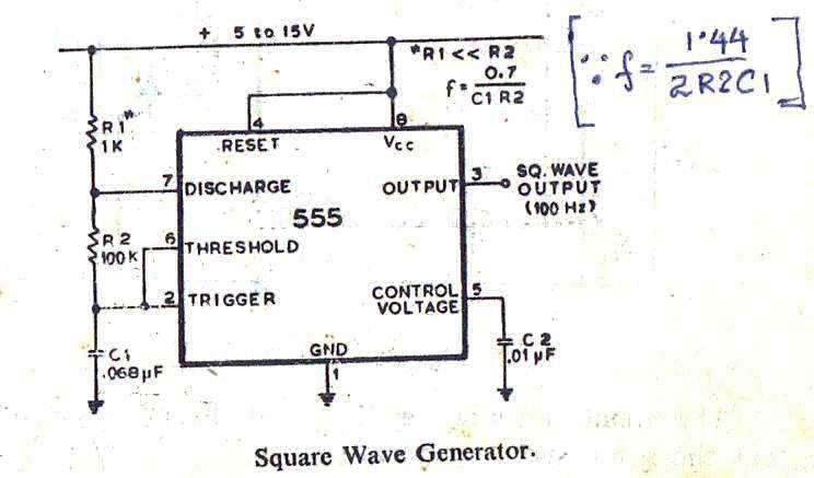
SQUARE WAVE OSCILLATOR USING 555IC

A Square waves can be obtained by using 555 timer IC by the circuit as shown in the figure below,


The asymmetry of a conventional astable circuit is a !result of the fact that charging and discharging times are not equal. In the circuit shown the capacitor Cl is charged through RI and R2 while discharged through R2. If Rl is made very small compared to R2, the.both time constant will be reduced so that they essentially depend on R2 and Cl, The frequency of operation (f) IS approximately 0.7/(R2C1). 

The frequency is of course independent to the supply voltage.

Photo Timer.


The circuit shown in Figure is useful for providing controlled 'on' times for such equipment as photo-enlargers, developers, small heaters, incandescent lamps, etc. Time is set by potentiometer R2 which provides a range of 1 sec. to 100 second with timing capacitor CI of 100 µF. 
The output at pin 3 is normally low and the relay is held off. A momentary touch on switch Sl energizes the relay which is held closed for a time 1.1 x (R1 + R2). C1 and then released. The exact length of the timing interval will depend on the actual capacitance of Cl. Most electrolytic capacitors are rated on the basis of minimum guaranteed value and the actual value may be higher. The circuit should be calibrated for various positions of the control knob of R2 after the timing capacitor has had a chance to age. Once the capacitor has reached its stable value, the timings provided should be well within the photographic requirements.

Touch Plate Controller


Touch the small metal plate and the relay gets energized, kept on for about 100 seconds and then released. Such circuits are ideally suited for making touch-operated call-bells, buzzers or small toys which, once touched, operate for a small time and then switch off automatically.
The input impedance of the trigger comparator of 555 is very high and the circuit can be triggered by the voltage induced in a human body. This fact is used in making the touch switch shown in Figure. Toy motors can be driven directly by deleting the diodes D1, D2 and the relay and driving a power transistor like AC 128 directly from the output pin 3 of the IC.


AUTO WIPER CONTROL


A continuously working wiper is a big nuisance when it is not raining hard. The wiper control shown in figure allows the wiper to sweep at rates varying from once a second to once in 10 second.
Basically the circuit is an astable multivibrator, in which the output level at pin 3 remains high for a long time decided by R2 and low for a short time decided by R3. The low going output at pin 3 drives the wiper motor via Tl and T2 for a time just sufficient to operate the parking switch. The wipers then make one sweep and rest again in their normal parked position till the next pulse. Resistor R5 limits the current and power dissipation in Tl. Transistors Tl and T2 may be replaced by a relay if desired.

AUTOMATIC HEADLIGHT TURN-OFF


Anyone who has stumbled around his dark garage after leaving his car for the night will appreciate this automatic head-light shut off switch. The switch, when installed in a car automatically turns off the headlights at pre-determined period after the ignition is switched off. In Figure when the ignition is first switched on,' the battery voltage is fed to the relay coil through diode D1. Switching off the ignition generates a negative-going pulse on pin.2 that triggers the timer. The output of the IC goes high to energise the relay and keep the headlights on long enough for you to leave the garage. With the values shown the delay is adjustable from approx. 10 seconds to 1 minute.


TINY FLASHER


A small size LED flasher operating on self contained batteries may be useful as a flashing metronome, dark room timer, memo¬ reminder and similar applications. The circuit of Figure is an astable multivibrator with a duty cycle of about 10%. LED connected as shown in the figure will be on for a short period and off for a longer period. The duty cycle will be reversed if R3 and the LED are connected as shown dotted in the figure and the battery consumption will also increase proportionally.